
About
The Consortium for the 3D printing of copper has grown quite organically out of several existing, and previously funded federal programs. There has been growing interest in the use of 3D Printing for the fabrication of particle accelerator components and vacuum electronics, complex heat exchangers, power electronics, power transfer, and induction welding tooling. Starting at the 2018 international vacuum electronics conference in Monterey, CA , and through our NAVSEA funded VED program (N0025316P0261), we formed a working group to guide further research efforts. What started as a handful of industry advisers quickly grew into a large group of companies. Leveraging this growing interest, and recognizing significant barriers (time and monetary) that no sole industrial or governmental entity is poised to address, we formed an officially recognized consortium. Its mission is to develop a set quality guidelines for AM OFE (Oxygen Free Electronic) grade copper and its feedstock materials including characterization of thermal, electrical, mechanical (quasi-static, fatigue, creep, high strain rate, etc.) properties as a function of melt parameters, bed temperature, powder size, grain size, oxygen content, orientation, geometry.
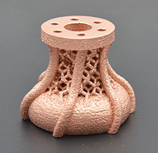
These applications require intricate designs and extensive metallurgical processing routes followed by assembly and brazing or welding of multiple components into a final part. Additive Manufacturing (AM) is rapidly changing the way in which many critical products are designed and manufactured, and in recent years has demonstrated the potential to disrupt cost-capability curve of copper components by eliminating manufacturing tooling, numerous piece parts, assembly, and high temperature joining operations. AM permits complex assemblies to be reduced to monolithic and mechanically robust structures, and enables new opportunities for advanced, high efficiency, three-dimensionally optimized designs and increased power handling capability with spatially optimized internal thermal management.
The underlying challenges associated with the additive manufacture of copper alloys, particularly for directed energy deposition (DED) and powder bed fusion (PBF) approaches, have been discussed in several recent studies and have also been reported in literature on copper welding. The very same properties inherent to copper that make it an ideal material for the aforementioned applications have severely limited its utilization in AM. The high thermal conductivity of copper rapidly conducts heat away from the melt pool producing local and global thermal gradients, residual stress accumulation, and distortion, is exacerbated by the significant difference in thermophysical properties between the consolidated material and the surrounding powder bed. Compounding these difficulties is the high reflectivity of copper at the wavelength of common Nd:YAG lasers used in many commercial PBF systems (~1060 nm) which often necessitates the use of high beam power resulting in increased recoil pressure, vaporization, spatter and related defects. During solidification this, coupled with the relatively low viscosity of molten copper, further promotes defects, solidification cracking, and porosity. For PBF and many other AM processes, it is also important to recognize that for many of the most suitable uses, the desirable properties of copper alloys are extremely sensitive to the deleterious effects of contamination, particularly by oxygen, which is difficult to control given the exceptionally large surface area of typical AM powder feedstock.
A notable result of these processing challenges, and perhaps the general lack of infrastructure and support for AM feedstock, equipment, and suitable process parameters, is that the use and deployment of copper in AM processes industrially is limited compared to other metals. Only in the past few years have these alloys been commercially demonstrated from a handful of sources, and publically available data regarding the performance and material properties from these sources are sparse. Literature on the subject is concentrated within the past 1-2 years, and with few exceptions, is focused predominantly on the investigation of processing feasibility, optimization of the process parameter space, or the demonstration of a noteworthy application. Among the published studies there generally exists little consensus on the optimal processing space, the resulting properties, or even the appropriate test methodology for determining the properties of AM copper which, due to specimen size limitations, often deviates significantly from standard practice. This gap suggests that as the demand and utilization of AM copper grows, new AM methodologies and approaches, specifically tailored for copper, will be required to address these scientific and engineering barriers, as well as to establish standards of measurement and best practices. Notwithstanding, the growing demand for AM solutions requiring the breadth of properties copper alloys offer has driven significant development efforts to improve copper alloy AM through improvement of feedstock materials, process parameters, process modeling, and material qualification.